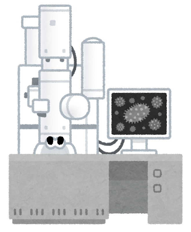
| Microstructural Characterization (Institute for Materials Research/The Electron Microscopy Center) |
|---|
| ■Technical support charge: 3,300 yen/hour ■Sample preparation room:330yen/hour |
| Equipment usage Charges【yen/day(8hours)】 |
| Equipment name | Open Project | Classified Project |
|---|---|---|
| SU8000,S-5500 | 14,080 | 72,160 |
| Titan80-300 | 36,080 | 106,480 |
| FEI-Titan G2-cubed | 46,640 | 121,440 |
| FEI-Titan G2-cubed | 50,160 | 125,860 |
※All charges listed here are including tax.
| Microstructural Characterization (Analytical Research Core for Advanced Materials) |
|---|
| ■Technical support charge: Open project:3,300 yen/hour Classified Project:6,600yen/hour |
| Equipment usage Charges【yen/day(8hours)】 |
| Equipment name | Open Project | Classified Project |
|---|---|---|
| JEM-ARM200F | 30,800 | 163,680 |
| Topcon EM-002B | 25,520 | 51,920 |
| JEOL JEM-2000EXII | 16,720 | 34,320 |
| FIB-SEM(Quanta 3D) | 30,360 | 62,920 |
| FIB-SEM(Versa 3D) | 30,360 | 62,920 |
| JEOL EM-09100IS | 17,600 | 32,560 |
| PIPSII | 9,680 | 22,880 |
| Model1010 | 3,520 | 13,200 |
| X-ray Diffractometer | 6,160 | 32,560 |
| Thermoanalysis | 5,280 | 12,320 |
※ All charges listed here are including tax.
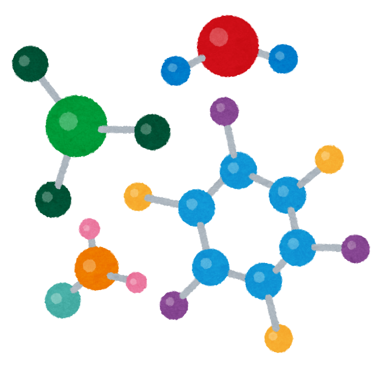
| Microstructural Characterization (Research and Analytical Center for Giant Molecules) |
|---|
| Equipment usage Charges【yen/day(8hours)】 |
| Equipment name | Open Project | Classified Project |
|---|---|---|
| Nuclear magnetic resonance (NMR) | 5,200 | 32,100 |
| ICP optical emission spectrometer | 3,200 | 4,600 |
・Raw chemicals for syntheses are not included.
・All charges listed here are including tax.
| Nanofabrication(MEMS) |
|---|
| 【Open Project】 ■Technical support fee: 3,300 yen/hour ■Facility usage charge: 960 yen/hour(790 yen/hour for the use within the Universityr ) 【Classified Project】 ■Technical support fee: 6,514 yen/hour ■Facility usage charge: 960 yen/hour(790 yen/hour for the use within the Universityr ) |
| No. | Equipment name | Open P | Classified P | No. | Equipment name | Open P | Classified P |
|---|---|---|---|---|---|---|---|
| A.Cleaning & drying | |||||||
| A-1 | Draft chamber | 1,290 | 1,548 | A-7 | Spin-drying machine | 2,428 | 2,914 |
| A-2 | Draft chamber for SiN etching | 1,730 | 2,076 | A-8 | Organic draft chamber | 1,290 | 1,548 |
| A-4 | Inert oven for sintering | 1,710 | 2,052 | A-9 | 4" spin drying machine | 2,612 | 3,134 |
| A-5 | Vacuum oven | 994 | 1,192 | A-10 | 6"spin drying machine | 2,612 | 3,134 |
| A-6 | Brush scrubber | 6,906 | 8,286 | ||||
| B.Photolithography | |||||||
| B-2 | Spin coater | 2,170 | 2,604 | B-13 | Elionix EB lithography | 9,422 | 11,306 |
| B-3 | Clean oven | 2,830 | 3,396 | B-14 | Laser writer | 7,094 | 8,512 |
| B-4 | Curing oven | 1,872 | 2,246 | B-15 | Maskless exposure system for ball | 4,450 | 5,340 |
| B-5 | Double-side aligner | 3,240 | 3,888 | B-16 | Spin dryer | 2,208 | 2,650 |
| B-8 | Draft chamber for development | 1,290 | 1,548 | B-17 | Hot plate | 994 | 1,192 |
| B-9 | UV curing | 4,120 | 4,944 | B-18 | maskless aligner | 5,374 | 6,450 |
| B-10 | Spin coater | 2,332 | 2,798 | B-19 | i-line stepper | 14,960 | 29,700 |
| B-11 | Spray developer | 2,156 | 2,588 | B-20 | Coater developer | 6,458 | 13,200 |
| C.Oxidation/diffusion, ion injection and heat treatment | |||||||
| C-1 | Oxidation furnace (for semiconductors)) | 10,598 | 12,716 | C-7 | Annealing furnace | 10,112 | 12,134 |
| C-2 | Oxidation furnace (for MEMS) | 9,168 | 11,000 | C-8 | Medium-current ion injector | 19,934 | 23,922 |
| C-3 | P diffusion furnace | 11,562 | 13,874 | C-10 | Rapid thermal annealing | 8,522 | 10,226 |
| C-4 | P push-in furnace | 9,854 | 11,824 | C-11 | Metal diffusion furnace | 7,856 | 9,426 |
| C-5 | B diffusion furnace | 10,938 | 13,126 | ||||
| C-6 | B push-in furnace | 9,854 | 11,824 | ||||
| D.Deposition | |||||||
| D-1 | LPCVD(SiN) | 12,108 | 14,530 | D-12 | MOCVD | 19,484 | 23,382 |
| D-2 | LPCVD(Poly-Si) | 11,838 | 14,206 | D-13 | JPEL PECVD | 15,156 | 18,188 |
| D-3 | LPCVD(SiO2) | 12,808 | 15,368 | D-14 | TEOS PECVD | 16,904 | 20,286 |
| D-4 | CVD | 21,326 | 25,590 | D-15 | Automatic Shibaura sputtering | 6,524 | 7,828 |
| D-5 | SUMITOMOSEIMITU PECVD | 15,350 | 18,420 | D-16 | Sputtering for ball | 4,392 | 5,270 |
| D-6 | W-CVD | 9,818 | 11,782 | D-17 | ALD | 10,418 | 12,502 |
| D-7 | ANELVA sputtering equipment | 8,588 | 10,306 | D-18 | High-temp. sputtering and O2 annealing | 11,698 | 14,038 |
| D-8 | SHIBAURA sputtering equipment | 3,758 | 4,510 | D-20 | ECR long-throw sputter | 6,450 | 7,740 |
| D-9 | Electron beam evaporator | 6,838 | 8,206 | D-21 | SPP Technologies TEOS PECVD | 16,770 | 21,507 |
| D-10 | Sol-gel auto-deposition system | 8,066 | 9,680 | ||||
| D-11 | Plating equipment | 2,534 | 3,040 | ||||
| E.Etching | |||||||
| E-1 | DeepRIE #1 | 8,054 | 9,666 | E-12 | TMAH etching equipment | 3,112 | 3,734 |
| E-2 | DeepRIE #2 | 8,054 | 9,666 | E-13 | DeepRIE #4 | 14,770 | 17,724 |
| E-3 | DeepRIE #3 | 8,278 | 9,934 | E-14 | Ion milling | 11,360 | 13,632 |
| E-4 | ANELVA RIE equipment | 7,078 | 8,494 | E-15 | Vapor HF etching | 8,534 | 10,240 |
| E-5 | ANELVA Si RIE equipment | 6,346 | 7,616 | E-16 | Ulvac ICP-RIE#1 | 15,970 | 19,166 |
| E-6 | Al-RIE | 11,912 | 14,294 | E-17 | Chemical Dry Etcher (CDE) | 5,976 | 7,172 |
| E-7 | ULVAC ashing equipment | 4,066 | 4,880 | E-18 | Plasma cleaner | 3,198 | 3,838 |
| E-8 | BRANSON ashing equipment | 3,316 | 3,980 | E-19 | Ulvac ICP-RIE#2 | 15,684 | 18,820 |
| E-10 | ULVAC multi-purpose RIE equipment | 10,902 | 13,082 | ||||
| E-11 | KOH etching equipment | 3,100 | 3,722 | ||||
| F.Bonding, polishing and packaging | |||||||
| F-1 | Wafer bonding equipment | 5,946 | 7,134 | F-9 | EVG wafer bonder | 6,112 | 7,336 |
| F-2 | TOKYO SEIMITSU dicer | 9,656 | 11,588 | F-10 | EVG aligner for wafer bonding | 5,302 | 6,362 |
| F-3 | DISCO dicer | 2,646 | 3,176 | F-11 | UV imprint | 6,638 | 7,964 |
| F-4 | Wire bonder | 1,186 | 1,424 | F-12 | Thermal imprint | 5,900 | 7,080 |
| F-5 | Laser marker | 2,436 | 2,922 | F-13 | Excimer lamp cleaner | 2,700 | 3,240 |
| F-6 | 6-inch wafer polishing equipment | 2,120 | 2,544 | F-14 | Surface planer | 14,974 | 17,968 |
| F-7 | 4-inch wafer polishing equipment | 1,822 | 2,186 | F-15 | Shibuya LAMICS AQL-1900 | 8,018 | 9,622 |
| F-8 | Sand blast | 3,418 | 4,102 | ||||
| G.Measurement | |||||||
| G-1 | Wafer dust detector | 1,976 | 2,372 | G-15 | Ultrasonic microscope | 2,284 | 2,742 |
| G-2 | Film thickness gage | 1,384 | 1,662 | G-16 | Digital thermo microscope | 1,248 | 1,496 |
| G-3 | Dektak step profiler | 1,658 | 1,990 | G-17 | Infrared microscope | 1,236 | 1,482 |
| G-4 | Tenchor step profiler | 1,658 | 1,990 | G-18 | Quadrupole mass analyzer | 1,226 | 1,472 |
| G-5 | Depth measuring equipment | 1,074 | 1,290 | G-20 | Quick coater | 1,338 | 1,606 |
| G-6 | 4-probe measuring equipment | 1,076 | 1,290 | G-22 | Desktop Ellipsometer | 746 | 896 |
| G-7 | Spreading resistance profiler | 2,616 | 3,140 | G-24 | Laser/white light conforcal microscope | 4,728 | 5,674 |
| G-8 | Wafer prober | 2,666 | 3,198 | G-25 | Line-focus-beam acoustic microscope for material characterization #1 | 3,488 | 4,184 |
| G-9 | Metal microscope | 1,152 | 1,382 | G-26 | Line-focus-beam acoustic microscope for material characterization #2 | 3,488 | 4,184 |
| G-10 | Digital microscope | 1,540 | 1,848 | G-27 | FIB | 9,596 | 11,516 |
| G-11 | Thermal electron SEM | 2,632 | 3,158 | G-28 | XRD | 5,154 | 6,184 |
| G-12 | FE-SEM | 4,622 | 5,546 | G-29 | JEOL FE-SEM | 5,330 | 6,396 |
| G-13 | Micro X-ray CT | 3,324 | 3,988 | ||||
| G-14 | Ellipsometer | 972 | 1,166 | ||||